Since 2009, W. L. Gore & Associates has partnered with technology leaders to develop custom reliable cables for lithography systems operating in ultra-clean and ultra-high vacuum environments. Our in-depth knowledge, materials expertise, cleaning processes and rigorous quality testing bring innovative cable assemblies for lithography applications that help our customers keep pace with the industry’s constantly evolving demands.
Lithography Products


EUV (extreme ultraviolet) and DUV (deep ultraviolet) lithography processes use light to transfer circuit patterns onto and carve electric circuits into silicon semiconductor wafers. Compared to DUV lithography, the shorter wavelength of EUV lithography allows more electric circuits to be squeezed onto a chip. Next-generation technology — High Numerical Aperture (High-NA EUV) lithography systems — will enable even finer lines and higher-density, higher-power chips. And this technology will demand even greater precision and purity every step of the way.
Gore can help meet these challenges facing lithography machine equipment manufacturers. We offer two categories of proven high-performance semiconductor cables for static and flexible applications. Both are qualified for high-vacuum environments. And both provide proven cleanliness, durability and reliability, enabling fabs to boost speeds and throughput without compromising yield, which can mean reduced maintenance, downtime and total costs over time.
You’ll find our reliable signal transmission cables in the wafer handling and exposure processes of the most advanced semiconductor lithography equipment. They’re also used in a variety of metrology and inspection equipment for automated wafer inspection, masks and chip quality.
We Customize. Without Compromise.
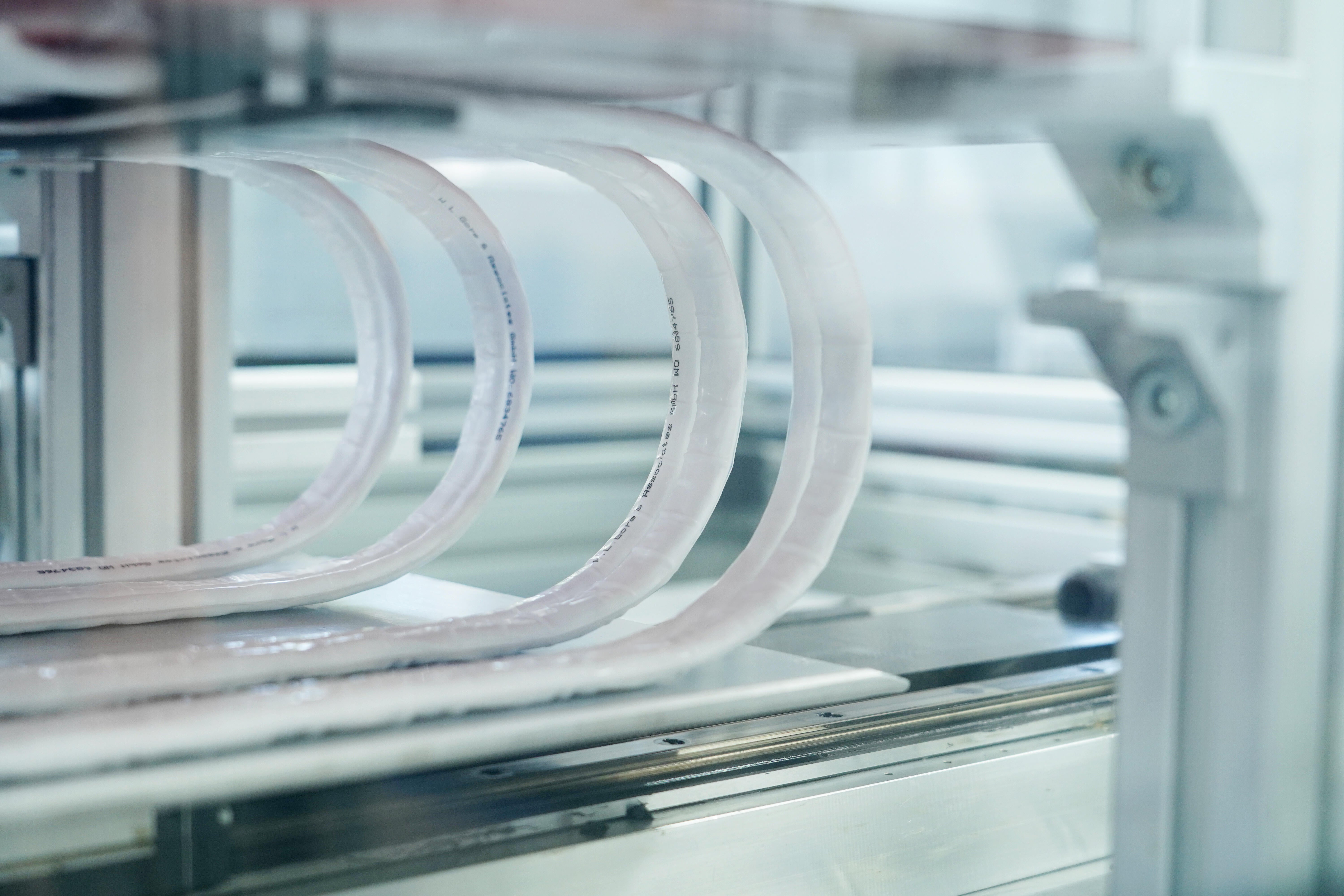
In the hands of our highly experienced teams, we customize without compromise. Each new project demonstrates our materials expertise and commitment to co-engineering. That’s because every Gore lithography cable is a custom, co-engineered product. We design, produce and quality-assure all of it — from our expanded polytetrafluoroethylene (ePTFE) jacketing material to the individual strands to the completed cable configuration, which may include more than a thousand strands.
Every material and element is tailored to specific customer requirements. We can fine-tune the characteristics of our ePTFE for the lowest particulation and lowest contamination for vacuum environments or other lithography-specific needs. And we continually evolve our methods and machinery in concert with the industry’s more demanding standards for cable cleanliness, durability, flex life and reliability.
From raw materials to finished assembly, Gore owns the process — and the responsibility to ensure our products perform as we say they will.
Gore Cable Solutions: For Lithography. For You.
Our ultra-clean, reliable cables and assemblies are custom-engineered to meet the challenges of more precision and cleanliness with higher yields, quality and speeds. These durable, high-performance lithography semiconductor cables have already been qualified in the most demanding Cleanliness Grade 1 high-vacuum environments, as well as in Cleanliness Grades 2 and 4 EUV and DUV applications. They also enable tight radius bends to facilitate easier installation and more flexible routing.
For static applications, we offer Cleanliness Grade 1 GORE® Ultraclean Static Round Cables & Assemblies. Our highest-purity cables can be found in the innermost parts of the equipment with the most extreme cleanliness requirements. Constructed with various fluoropolymers — including Gore’s ePTFE — they start with low outgassing values, which we can tailor to even lower levels to meet your specific requirements.
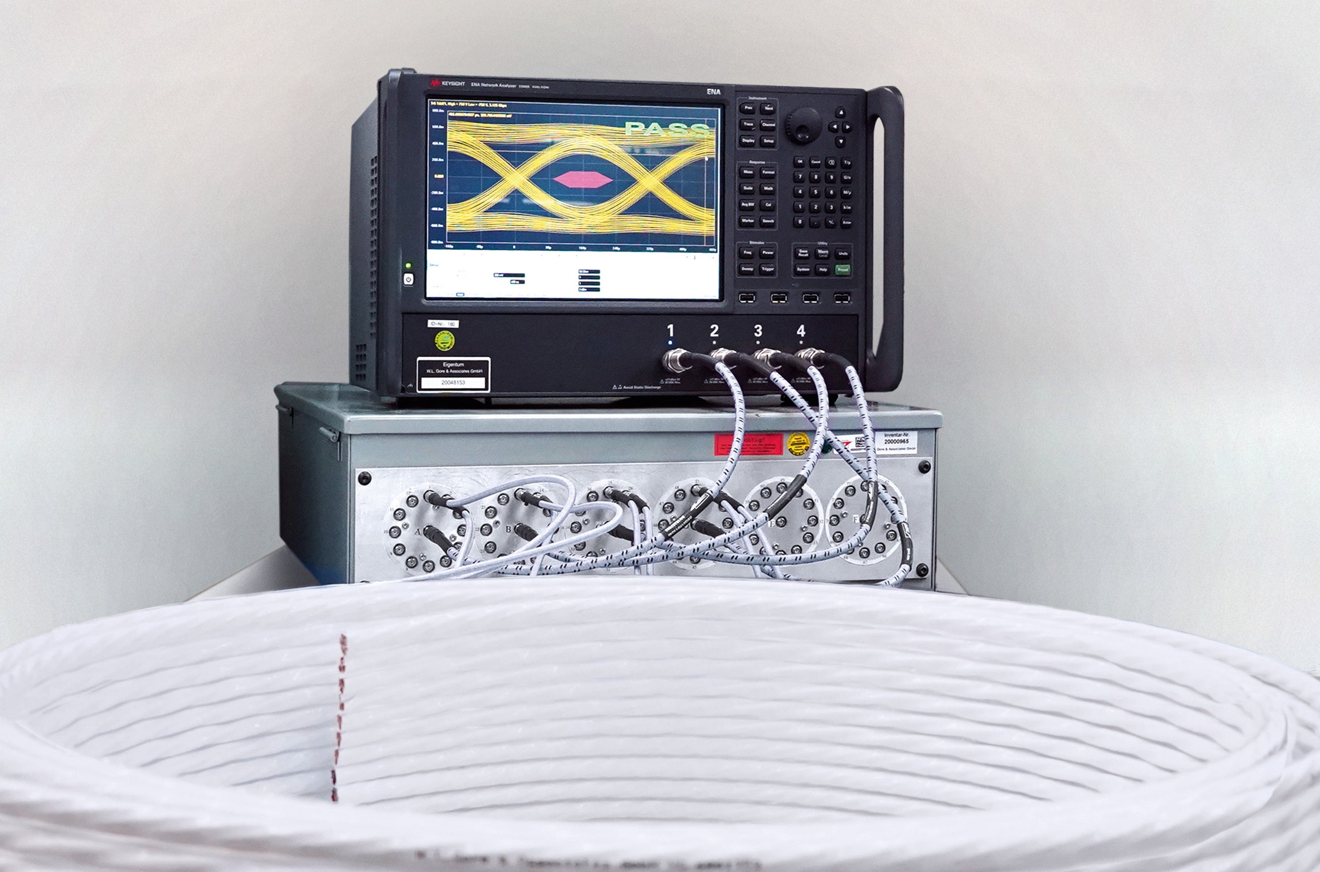
For EUV and DUV applications, Cleanliness Grades 2 and 4 GORE® High Flex Cables & Assemblies provide reliable performance and purity even under higher-speed, higher-stress multi-million flex cycles. With proven durability in complex environments where other cables fail, our low-outgassing high-flex vacuum cables are engineered for improved signal integrity and transmission speeds. These are crucial features for complicated configurations of EUV and DUV cables incorporating tubes for gas or fluid transport alongside cabling for data and high- and low-power electrical signals.
Get Started with Gore Lithography Cables
Why choose Gore? Because we offer lithography semiconductor companies high-quality cables that translate to real value in use with less maintenance and downtime for lower total costs over the equipment’s lifecycle. We design, engineer and manufacture our cables to meet the lithography industry’s toughest standards for durability, outgassing performance, cleanliness and flexibility. They’re proven to deliver the lowest contamination, lowest particulation and more reliable signal integrity for high-purity lithography services or vacuum applications.
To learn more and talk to us about customizing cables that meet your specific lithography, metrology and inspection equipment needs and requirements, contact a Gore specialist today.
FOR INDUSTRIAL USE ONLY
Not for use in food, drug, cosmetic or medical device manufacturing, processing, or packaging operations.
Contact Us
United States
+1 800 356 4622
Germany
+49 9144 6010
+49 9144 6816 (fax)
UK
+44 1382 56 1511
+44 1382 56 1007 (fax)
Italy
+39 045 6209 209
+39 045 6209 165 (fax)
France
+33 1 5695 6565
+33 1 5695 6401 (fax)
Spain
+34 93 480 6900
+34 93 373 7850 (fax)
Sweden
+46 31 7067800
+46 31 864226 (fax)
China (Beijing)
+86 10 5707 4999
+86 10 5707 4900 (fax)
China (Shanghai)
+86 21 5172 8299
+86 21 6247 9199 (fax)
China (Shenzhen)
+86 755 8359 8262
+86 755 8359 1654 (fax)
South Korea
+82 2 393 3411
+82 2 393 1285 (fax)
Japan
+81 3 6746 2582
+81 3 6746 2571 (fax)